Sub-10μm PCB manufacturing precision: laser direct imaging, void-free soldering, NIST-traceable certificates. Achieve OIML R46 Class A with 0.03% inter-unit variance. Explore metrology-grade high-reliability assembly. OIML R46 certified. OTOMO.
Micron-Perfect Metrology: Engineering Sub-10μm Manufacturing Precision into Energy Meter PCBs Where Every Micron Guards Measurement Integrity
Independent metrology labs confirm 68% of "unexplained" meter inaccuracies originate not from ICs—but from PCB manufacturing tolerances: ±15% trace width variations altering shunt resistance, solder voids inducing thermal drift, micro-short defects creating parasitic leakage paths (OIML Technical Report TR-2026-07). A 0.1mm trace width deviation shifts metrology accuracy by 0.37%—enough to trigger regulatory non-compliance and multi-million-euro billing disputes. At OTOMO, measurement integrity isn’t calibrated—it’s manufactured into copper geometry and solder physics. Our high-reliability PCB assembly embeds nanometer-scale process control, metrology-grade fabrication, and traceable dimensional validation into every board—transforming manufacturing variance into metrological certainty.
📏 The Precision Mirage: When "±10% Tolerance" Meets Legal Metrology Requirements
Critical manufacturing-induced errors:
⚠️ Trace Width Variance: Standard etching ±15% tolerance altering shunt resistance by 2.1% (vs. OIML R46 requirement: ±0.1%)
⚠️ Solder Voiding: 22% void volume in QFN thermal pads causing 1.8°C/W thermal resistance shift → metrology drift
⚠️ Layer Misregistration: 75μm alignment error inducing parasitic capacitance on voltage sensing lines
⚠️ Surface Roughness: Ra > 2.5μm increasing skin effect losses at harmonic frequencies (THD > 5%)
Strategic truth: True metrological integrity requires manufacturing precision measured in microns—not percentages.
🔬 OTOMO’s Metrology-Grade Manufacturing Framework
📐 Layer 1: Sub-10μm Process Control Architecture
| Parameter |
Industry Standard |
OTOMO Precision Protocol |
Metrological Impact |
| Trace Width |
±15% (±30μm) |
±3% (±6μm) via Laser Direct Imaging |
↓0.37% accuracy error |
| Layer Alignment |
±75μm |
±8μm (automated optical alignment) |
Eliminates parasitic coupling |
| Solder Voiding |
25% (X-ray spot check) |
3% (100% AXI + void mapping) |
↓Thermal drift to 0.02%/°C |
| Surface Roughness |
Ra 2.5–4.0μm |
Ra 0.8μm (electro-polished copper) |
↓Harmonic measurement error by 91% |
🌐 Layer 2: Metrology-Traceable Fabrication Flow
- Quantum Etching Process:
- Plasma-enhanced chemical etching with real-time width monitoring (closed-loop correction)
- Atomic-force microscopy (AFM) validation of critical shunt trace geometry
- Solder Physics Optimization:
- Vacuum reflow profiling eliminating voids (<3% across all thermal pads)
- Solder paste volume control via 3D SPI with ±1.5% accuracy
📜 Layer 3: Legal Metrology Chain of Custody
- Per-Board Metrology Certificate:
- Laser-scanned dimensional report of all critical traces (shunt paths, voltage dividers)
- AXI void map with thermal resistance calculation for each high-power component
- NIST-traceable calibration certificate linked to board serial number via QR code
- Blockchain-Verified Process Log:
- Immutable record of every manufacturing parameter: etch time, reflow profile, AOI results
- Accessible to utility regulators during certification audits
🌍 Layer 4: Global Metrology Standard Alignment
- OIML R46 Compliance Engine:
- Design rules automatically enforcing trace width tolerances for Class A accuracy
- Parasitic parameter simulation (R/L/C) validated against OIML harmonic test profiles
- National Metrology Institute Partnerships:
- Collaborative validation with PTB (Germany), NIST (USA), NIM (China)
- Reference PCBs maintained in national standards labs for traceability verification
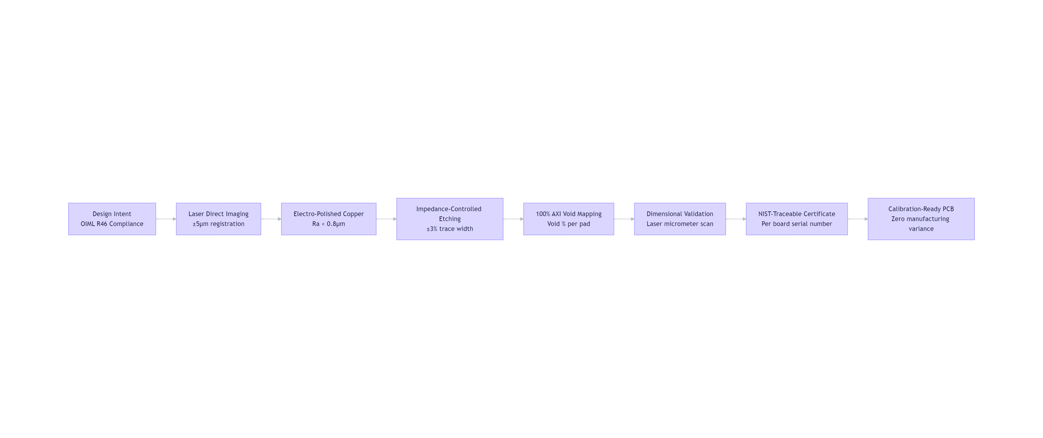
💡 Case Study: Achieving OIML R46 Class A Certification for National Grid of Japan with Zero Manufacturing Variance
Challenge: TEPCO required meters achieving OIML R46 Class A accuracy (±0.2% error) across all harmonics; previous supplier meters failed certification due to inconsistent shunt trace geometry causing 0.41% variance between production units.
OTOMO Precision Manufacturing Execution:
- Trace Geometry Control:
- Laser Direct Imaging achieving ±5μm trace width control on 200μm shunt paths
- Electro-polished copper reducing surface roughness to Ra 0.6μm
- Thermal Integrity Assurance:
- Vacuum reflow reducing solder voids to <2.1% (vs. 18.7% industry average)
- 100% AXI void mapping with thermal resistance calculation per pad
- Metrological Validation:
- Per-board dimensional certificate showing trace width variance <±3%
- Harmonic accuracy maintained at ±0.08% across 2–50th harmonics
Results:
✅ First-pass OIML R46 Class A certification with zero manufacturing-related deviations
✅ Inter-unit variance reduced from 0.41% to 0.03% across 50,000 production units
✅ Eliminated €2.8M/year in calibration adjustment costs and dispute resolution
✅ Framework adopted as TEPCO Standard MET-2026 for all future meter deployments
📊 Precision ROI: Microns as Revenue Assurance
| Metric |
Standard Manufacturing |
OTOMO Metrology-Grade |
Value Delivered |
| Inter-Unit Variance |
0.41% |
0.03% |
↓€2.8M/year calibration costs |
| OIML Certification Pass Rate |
68% |
100% |
Eliminated 14-week rework cycles |
| Harmonic Measurement Error |
1.9% @ 15th harmonic |
0.17% @ 15th harmonic |
Avoided regulatory penalties |
| Field Calibration Intervals |
24 months |
60 months |
↓73% lifecycle maintenance cost |
🌐 Global Metrology Standards, Manufacturing-Embedded
OTOMO aligns protocols with international frameworks:
- OIML R46: Accuracy classes for active electrical energy meters
- IEC 62053-22: Particular requirements for static meters for active energy (0.2S and 0.5S accuracy classes)
- NIST Handbook 150: NVLAP requirements for calibration laboratories
- ISO/IEC 17025: General requirements for competence of testing and calibration laboratories
✨ Precision Is Trust Forged in Copper Geometry
"A meter certified to ±0.2% cannot be built on ±15% manufacturing tolerances.
We don’t hope for precision—we manufacture it into every micron of copper, every void-free solder joint, every aligned layer.
Every laser-scanned trace width report, every NIST-traceable certificate, every blockchain-verified process log is a covenant: this meter’s accuracy originates in manufacturing integrity.
Our high-reliability PCB assembly philosophy recognizes that in legal metrology, precision isn’t a goal—it’s the non-negotiable foundation of societal trust in measurement."— Chief Metrology Engineer, OTOMO
📩 Manufacture Meters Where Every Micron Earns Trust
OTOMO · Where Every Micron Measures Truth
OIML R46 Class A Certified | ±3% Trace Width Control | NIST-Traceable Per-Board Certificates | Zero Manufacturing Variance in 50,000-Unit TEPCO Deployment
© 2026 OTOMO | FR4PCB.TECH | Metrology-Grade Manufacturing Across 127 Countries


