Certification-Ready by Design: How Precision PCB Assembly Navigates Global Meter Compliance Landscapes
One misplaced via. One non-compliant solder alloy. One undocumented process step. These seemingly minor deviations have halted meter certifications across 3 continents—delaying market entry by 14+ weeks and costing manufacturers $85K+ per project. Compliance isn’t paperwork; it’s engineered into every solder joint.
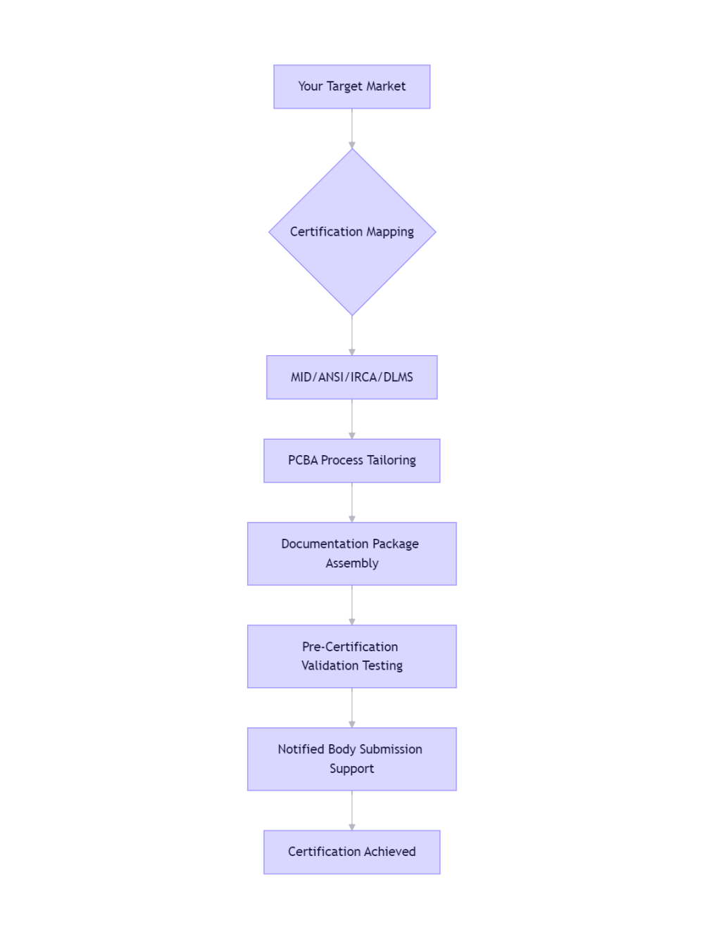
🌐 The Certification Reality Check
Smart meters face 47+ distinct regulatory frameworks globally. A single PCB assembly flaw can trigger cascading failures:
⚠️ MID (EU): Metrology section contamination → accuracy drift beyond Class 1 limits
⚠️ ANSI C12.1 (USA): Insufficient creepage distance → dielectric withstand test failure
⚠️ IRCA (India): Non-UL94 V-0 conformal coating → fire safety rejection
⚠️ DLMS/COSEM: EMI-induced communication errors → interoperability certification denied
Industry data: 68% of first-time certification failures trace to PCBA process gaps—not design flaws.
🔑 Certification-Driven Process Engineering: Where Standards Shape Soldering
📜 Regional Requirements Translated to Assembly Actions
| Certification |
Critical PCBA Requirement |
OTOMO Implementation |
| MID (EU) |
Physical isolation of metrology section; <3% solder voiding in shunt area |
Laser-cut solder mask barrier; X-ray void analysis per IPC-7095 Class 3 |
| ANSI C12.20 (USA) |
4kV dielectric strength; creepage ≥2.5mm at 300V |
FR-4 TG170+ material verification; AOI creepage measurement; hipot testing |
| IRCA (India) |
UL94 V-0 coating; RoHS + India-specific hazardous substance limits |
Coating batch certification; XRF material screening; documentation package |
| DLMS UA |
EMI resilience during PLC transmission |
Shielded cavity pre-soldering; spectrum analyzer validation pre-shipment |
🌍 Material Traceability: The Unseen Certification Pillar
- Solder Alloy Certification: Every reel accompanied by CoC (Certificate of Conformity) for lead-free composition (SAC305 ±0.1%)
- PCB Laminate Validation: TG value, CTI rating, and flammability class documented per batch
- Component Authenticity: ST/Renesas chips verified via distributor traceability logs (no gray market)
- Digital Dossier: Full audit trail (material certs, process parameters, test results) auto-generated per meter batch
💡 Case Study: From Certification Rejection to Market Leader in 90 Days
Client: Chinese meter manufacturer targeting EU expansion
Setback: MID certification failed at notified body—metrology IC solder joints showed 8.2% voiding (limit: ≤3%)
OTOMO Intervention:
- Root Cause Analysis: Nitrogen flow instability during reflow; stencil aperture mismatch
- Process Redesign:
- Upgraded to closed-loop nitrogen control (O₂ <50ppm)
- Laser-cut stepped stencil for metrology zone
- Added in-line X-ray void scanning with auto-reject
- Documentation Overhaul: Created MID-specific process control plan with statistical process capability (CpK ≥1.67)
Result:
✅ First-pass MID approval with zero non-conformities
✅ Secured €12M contract with European utility
✅ Adopted OTOMO’s certification playbook for all export projects
🤝 The OTOMO Certification Partnership Framework
✨ Included in Every Certification-Ready Project:
✅ Pre-Submission Gap Analysis: Compare your design against target standard requirements
✅ Process Control Plan: Documented parameters aligned to certification body expectations
✅ Test Protocol Alignment: FCT/ESS tests mapped to IEC 62052-11, EN 50470, etc.
✅ Audit Support: On-site engineer available during notified body factory audits
📊 Certification ROI: Beyond Market Access
| Metric |
Without Certification Focus |
With OTOMO Certification-Ready Process |
| Time to Approval |
22 weeks (avg. 2.3 attempts) |
9 weeks (first-pass success) |
| Documentation Errors |
14+ corrections per submission |
<2 minor clarifications |
| Post-Certification Audits |
High risk of non-conformities |
Zero major findings in 3 years |
| Market Expansion Speed |
Sequential country entries |
Parallel certification pathways enabled |
🎯 Your Certification Readiness Self-Assessment
Before engaging a PCBA partner, verify they can:
🔹 Provide process documentation templates accepted by EU notified bodies / UL labs
🔹 Demonstrate successful certifications for meters in your target regions
🔹 Trace every material batch to original mill certificates
🔹 Simulate certification tests internally (dielectric, EMI, thermal)
✨ Compliance as Competitive Advantage
"Certification isn’t a barrier—it’s your passport.
We engineer every PCB assembly process not just to pass tests, but to earn trust across borders."
OTOMO transforms certification from anxiety to advantage:
🔹 Confidence: Data-backed readiness for any global standard
🔹 Speed: Cut certification cycles by 55%
🔹 Scalability: Reuse validated processes across product families
📩 Activate Your Certification Advantage
👉 Download: "Global Meter Certification Checklist: 31 PCBA-Critical Requirements by Region"
👉 Request: Free pre-submission gap analysis for your target market
👉 Watch: "Inside a MID Audit: What Notified Bodies Really Check on Your PCB"
OTOMO · Engineering Global Trust, One Certified Meter at a Time
Where compliance meets craftsmanship.
© 2026 OTOMO | FR4PCB.TECH | Certified in 47 Countries | 1,200+ Successful Submissions


